PowDeR/RF Power Devices
Home - Projects - Publications - Staff - Lab Capabilities - Thesis
WORK IN PROGRESS!
10 GHz RF Power Amplifier for Continuous Wave Load Pull measurements
Introduction
We developed a custom rackmount amplifier capable of delivering a RF continuous power of 8W on a 50-ohm load at a nominal frequency of 10GHz. The amplifier has been integrated into an existing on-wafer 2GHz CW RF Load Pull measurement system, thus extending its performace capabilities to the frequency of 10GHz , and is based on commercial amplifier modules, all manufactured by Kuhne Electronic GmbH, Germany, [1].
System description
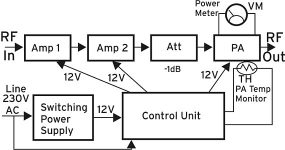
The system consists of a cascade of three amplifier modules, Amp1, Amp2 and PA, as shown in Fig.1.
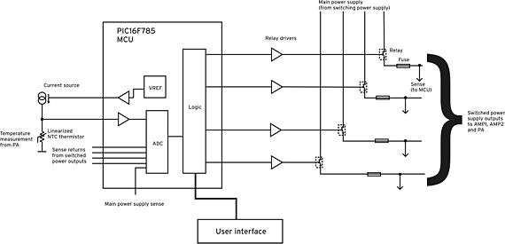
The signal to be amplified (RF In) is used to feed the pre-amplification chain Amp1 – Amp2. These amplifiers (Kuhne P/N: MKU PA 102AL) are characterized by a nominal gain of 18.5dB and maximum saturated power 300mW. The output of Amp2 is fed into PA through a 2W 1dB attenuator, Att (Aeroflex Inmet P/N: 18AH-01, USA). The purpose of such attenuator is to prevent the signal at the input of the power amplifier PA from exceeding 300mW under any working condition, which is the absolute maximum power that can be fed into PA. The power amplifier PA (Kuhne P/N: MKU PA 102XL) is designed to work at the nominal frequency of 10GHz and is capable of yielding a maximum saturated power of 12W and a nominal gain of 20.7dB. The signal chain from RF In to RF Out is thus characterized by a typical RF gain of 56.7dB. The power amplifier PA has an auxiliary output providing a voltage proportional to the output power. Such voltage has been used to feed a power meter VM based on a LED bargraph. All the amplifiers have a separate supply line (+12V nominal), and PA has two: one to bias the gates of the active devices inside and one for the drains. All the amplifiers have to be powered up and down in a correct sequence to ensure that no damage is inflicted to the system under any operating condition. Also, the temperature of the PA is never to exceed 55°C, so a temperature measurement circuit was considered to be mandatory. For such purposes a control unit has been custom developed based on a microcontroller. The block diagram of the control unit is sketched in Fig. 2.
The control unit is based on a PIC microcontroller MCU (Microchip Tech. P/N: PIC16F785, USA), which is a feature-rich unit incorporating a bandgap reference voltage, a 10-bit ADC, two configurable rail-to-rail op-amps plus timers and comparators. The aim of the control unit is to provide the correct power-on and power-off sequence to the amplification chain (AMP1, AMP2 and PA) with the correct timings to ensure that an amplifier in the chain is powered only after the previous one is fully on. Supply to amplifiers is provided by the switching power supply unit (Kuhne P/N: S-150-W-12). Each supply line output is switched on and off by means of a relay, and it independently fused. Separate power sense lines are provided to each supply line to detect failures. These sense returns, along with the main supply line, are continuously acquired by the analog-to-digital converter onboard the MCU in order to ensure that the voltages fed to the amplification chain are within the recommended limits at all times. In order to measure the operating temperature of the PA module, a temperature monitor has been inluded into the design based on a linearized NTC thermistor biased by a constant current controlled by the reference voltage inside the MCU . The voltage across the NTC is then amplified and acquired by the ADC onboard the microcontroller. The aim of the temperature monitor is to make sure that the PA temperature never exceeds 55°C, which is the absolute maximum operating temperature of the module according to the manufacturer’s specifications. For safety reasons, the control unit powers off the amplification chain at a temperature of 53°C at the PA. A simple user interface with a switch and two LEDs gives the user information about the status of the system. Distinctive blinking sequences of LEDs “OK” and “°C” describe the type of fault occurred, e.g. an overtemperature, a blown fuse, a faulty relay or an abnormal voltage at the switched supply lines. In such cases, the amplification chain is turned off in the correct sequence and, by recognizing the blinking sequence, the user is able to determine among the supply lines the one that is faulty. When everything is ok LED “OK” is lit and “°C” is off. Other safety features include the power up prevention of the system if the PA temperature is over 39°C, or if the voltages at the main supply line are not within the upper and lower bounds. In this case the control unit informs the user when it is possible to power up the system again. An additional LED “Operate” is lit when the amplification chain is fully on. The main switch is key-operated and is located on the rear panel. By turning such switch to on the user powers up the switching power supply and the control unit. The amplification chain is powered up by switching the front panel switch from the “Standby” position to the “Operate” position.
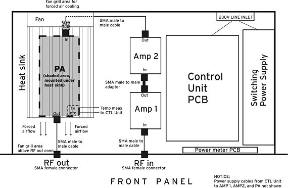
Fig.3 shows the assembly layout of the instrument.
The system is housed into a three-unit-high, 19 in. rackmount case (Schroff, Germany). The amplifier modules are interconnected by means of semi-flexible SMA cables (all manufactured by Tensolite, USA). Amp 1 and Amp 2 are interconnected by means of a standard SMA male-to-male adapter. A 0.21°C/W heatsink (Kuhne P/N: SK150-62) is used to cool the PA module by means of forced air provided by a fan (Kuhne P/N: FAN 80x80 12V). The PA is mounted below the heatsink and the heat transfer between them is enhanced by the use of thermally conductive paste.
System characterization
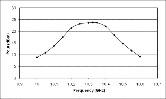
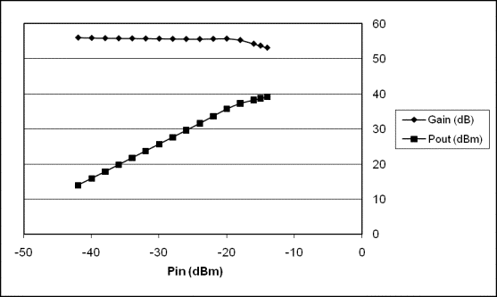
The optimum working frequency of the amplifier has been determined based on the maximum power output with a fixed amplitude frequency sweep at the amplifier input. Fig. 4 shows the amplifier response to an input frequency sweep at a fixed amplitude of –32dBm.
According to Fig. 4, the system displayed a peak response at the frequency of 10325MHz. Such value is henceforth considered to be the optimum working frequency of the amplifier. The characterization of the amplifier in terms of gain and output power, both displayed in Fig. 5, was carried out at such frequency. An output power of about 8W was observed in saturation conditions.
Images
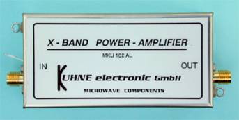
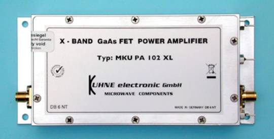
Fig. 6 and Fig. 7 show an image of the amplifiers AMP1-2 and PA respectively.
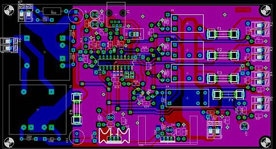
Fig.8 depicts the layout of the control unit PCB, a double sided-PCB. Red tracks are routed on the component side of the board, blue tracks are routed on the solder side.
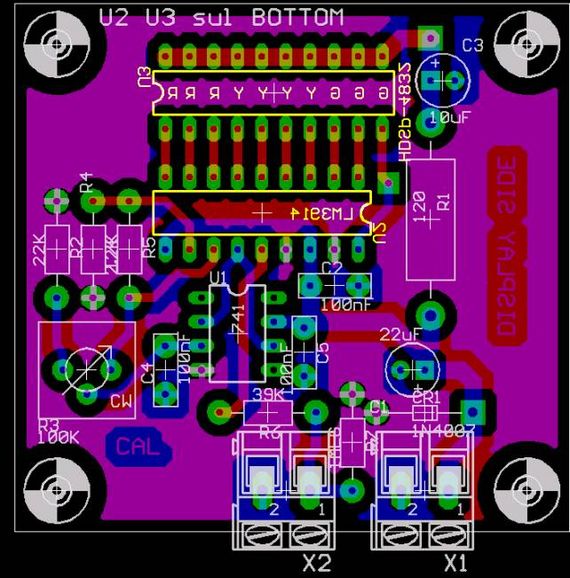
Fig. 9 displays the layout of the power meter board, based on a LED bargraph.
Fig. 10 is a front view of the amplifier, installed into a CW RF Load Pull measurement system.

