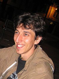
Luca Morassi: Difference between revisions
No edit summary |
No edit summary |
||
| Line 1: | Line 1: | ||
[[File:MyPic.JPG|left]]Ph.D. Student | [[File:MyPic.JPG|200px|left]]Ph.D. Student | ||
Course: Electronics and Telecommunications | Course: Electronics and Telecommunications | ||
---- | ---- | ||
Revision as of 15:03, 23 December 2010
Ph.D. Student
Course: Electronics and Telecommunications
Brief CV:
Luca Morassi was born in Mirandola (Mo), Italy, on September 15th, 1982.
From July 2008 to February 2009 he was in IMEC (Interuniversity MicroElectronics Centre, Leuven, Belgium) for an internship; during this period he worked on the characterization of High-k-based composed stack for MOSFETs (Metal Oxide Semiconductor Field Effect Transistor) gate oxide. In 2009 he received his academic master degree in Electronic Engineering from University of Modena e Reggio Emilia, Italy - Topic: "Characterization and Simulation of High-k Dielectrics for Innovative Non-Volatile Memories". During 2009 he collaborated with University of Modena and Reggio Emilia with a research activity focused on the electrical characterization of high-k material for Non-Volatile Memory (NVM) devices. Since 2010 he is a PhD student at ICT Electronics & Telecommunications Doctorate School, Modena, Italy with a research activity based on III-V compound semiconductor. His main research field is the characterization of InGaAs-channel MOSFETs and MOSHEMTs (Metal Oxide Semiconductor High Electron Mobilty Transistors) for high power and logic applications.
List of publications and papers in international conference:
A. Padovani, L. Morassi, N. Raghavan, L. Larcher, L. Wenhu, K. L. Pey, and G. Bersuker", A Physical Model for Post-Breakdown Digital Gate Current Noise", Electr. Dev. Lett., vol. 31, no. 9, pp.1032-1034, Sep. 2010.
L. Morassi, L. Larcher, L. Pantisano, A. Padovani, R. Degreave, M. B. Zahid, and B. J. O'Sullivan, "Advanced high-k materials and electrical analysis for memories: the role of SiO2-high-k dielectric intermixing", 41th International Conference on Solid State Devices and Materials (SSDM2009), Sendai, Japan, 2009.
G. Bersuker, D. Heh, C. D. Young, L. Morassi, A. Padovani, L. Larcher, K. S. Yew, Y. C. Ong, D. S. Ang, K. L. Pey, and W. Taylor, "Mechanism of high-k dielectric-induced breakdown of interfacial SiO2 layer", IEEE International Reliability Physics Symposium, Anaheim (CA), USA, May 2-6, 2010, pp. 373-378.
G. Bersuker, D. Veksler, C. D. Young, H. Park, L. Morassi, A. Padovani, L. Larcher, W. Taylor, P. D. Kirsch, and R. Jammy, "Connecting electrical and structural dielectric characteristics", Advanced Workshop on 'Frontiers in Electronics' (WOFE 2009), Puerto Rico, December 13-16, 2009.
L. Morassi, G. Verzellesi, A. Padovani, L. Larcher, P. Pavan, D. Veksler, I. Ok, and G. Bersuker, "Analysis of interface-trap effects in inversion-type InGaAs/ZrO2 MOSFETs", IEEE International Reliability Physics Symposium, Anaheim (CA), USA, May 2-6, 2010, pp. 532-535.
L. Morassi, A. Padovani, G. Verzellesi, D. Veksler, I. Ok and G. Bersuker, “Study of the Impact of Interface Traps on the Electrical Characteristics of InGaAs-based MOSFETs and MOSHEMTs with high-k Gate Dielectrics”, 19th European Workshop on Heterostructure Technology (HETEC2010), Crete, Greece, Oct 18-20, 2010.
L. Morassi, A. Padovani, G. Verzellesi, D. Veksler, I. Ok, G. Bersuker, "Interface-Trap Effects in Inversion-Type Enhancement-Mode InGaAs/ZrO2 N-Channel MOSFETs", Accepted for publication Trans. on Electr. Dev..
Scientific activities:
Partecipation at the conference: IEEE International Reliability Physics Symposium; oral presentaion of the work:
L. Morassi, G. Verzellesi, A. Padovani, L. Larcher, P. Pavan, D. Veksler, I. Ok, and G. Bersuker, "Analysis of interface-trap effects in inversion-type InGaAs/ZrO2 MOSFETs", IEEE International Reliability Physics Symposium, Anaheim (CA), USA, May 2-6, 2010, pp. 532-535.
Partecipation at the conference: European Workshop on Heterostructure Technology; oral presentaion of the work:
L. Morassi, A. Padovani, G. Verzellesi, D. Veksler, I. Ok and G. Bersuker, “Study of the Impact of Interface Traps on the Electrical Characteristics of InGaAs-based MOSFETs and MOSHEMTs with high-k Gate Dielectrics”, 19th European Workshop on Heterostructure Technology (HETEC2010), Crete, Greece, Oct 18-20, 2010.
DISMI - Dipartimento di Scienze e Metodi dell'Ingegneria
Università di Modena e Reggio Emilia
Pad. Tamburini - Via Amendola 2
42122, Reggio Emilia
mail: luca.morassi@unimore.it
Tel: +39-0522522638
Fax: +39-0522522609
Cell: +39-3381468756
