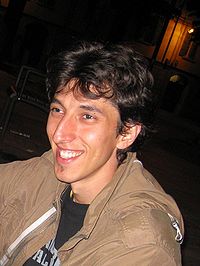
Luca Morassi
Ph.D. Student
Course: Electronics and Telecommunications
Brief CV:
Luca Morassi was born in Mirandola (Mo), Italy, on September 15th, 1982.
From July 2008 to February 2009 he was in IMEC (Interuniversity MicroElectronics Centre, Leuven, Belgium) for an internship; during this period he worked on the characterization of High-k-based composed stack for MOSFETs (Metal Oxide Semiconductor Field Effect Transistor) gate oxide. In 2009 he received his academic master degree in Electronic Engineering from University of Modena e Reggio Emilia, Italy - Topic: "Characterization and Simulation of High-k Dielectrics for Innovative Non-Volatile Memories". During 2009 he collaborated with University of Modena and Reggio Emilia with a research activity focused on the electrical characterization of high-k material for Non-Volatile Memory (NVM) devices. Since 2010 he is a PhD student at ICT Electronics & Telecommunications Doctorate School, Modena, Italy with a research activity based on III-V compound semiconductor. His main research field is the characterization of InGaAs-channel MOSFETs and MOSHEMTs (Metal Oxide Semiconductor High Electron Mobilty Transistors) for high power and logic applications.
List of publications in journals:
[J1] Padovani, A.; Morassi, L.; Raghavan, N.; Larcher, L.; Wenhu Liu; Kin Leong Pey; Bersuker, G.; , "A Physical Model for Post-Breakdown Digital Gate Current Noise," Electron Device Letters, IEEE , vol.31, no.9, pp.1032-1034, Sept. 2010
[J2] Morassi, L.; Padovani, A.; Verzellesi, G.; Veksler, D.; Injo Ok; Bersuker, G.; , "Interface-Trap Effects in Inversion-Type Enhancement-Mode N-Channel MOSFETs," Electron Devices, IEEE Transactions on , vol.58, no.1, pp.107-114, Jan. 2011
[J3] Bersuker, G.; Veksler, D.; Young, C.D.; Park, H.; Taylor, W.; Kirsch, P.; Jammy, R.; Morassi, L.; Padovani, A.; Larcher, L.; , “Connecting electrical and structural dielectric characteristics,” International Journal of High Speed Electronics and Systems (IJHSES), vol. 20(1), pp. 65-79, 2011
[J4] Morassi, L.; Verzellesi, G.; Zhao, H.; Lee, J. C.; Veksler, D.; Bersuker, G.; , "Errors Limiting Split-CV Mobility Extraction Accuracy in Buried-Channel InGaAs MOSFETs," Electron Devices, IEEE Transactions on , vol.59, no.4, pp.1068-1075, April 2012
[J5] Morassi, L.; Verzellesi, G.; Zhao, H.; Lee, J. C.; Veksler, D.; Bersuker, G.; , "Engineering Barrier and Buffer Layers in InGaAs Quantum-Well MOSFETs," Electron Devices, IEEE Transactions on , vol.59, no.12, pp.3651-3654, Dec. 2012
List of publications in international conferences:
[C1] Morassi, L.; Larcher, L.; Pantisano, L.; Padovani, A.; Degreave, R.; Zahid, M. B.; O'Sullivan, B. J.; , "Advanced high-k materials and electrical analysis for memories: the role of SiO2-high-k dielectric intermixing," 41th International Conference on Solid State Devices and Materials (SSDM2009), Sendai, Japan, 2009
[C2] Bersuker, G.; Heh, D.; Young, C.D.; Morassi, L.; Padovani, A.; Larcher, L.; Yew, K.S.; Ong, Y.C.; Ang, D.S.; Pey, K.L.; Taylor, W.; , "Mechanism of high-k dielectric-induced breakdown of the interfacial SiO2 layer," Reliability Physics Symposium (IRPS), 2010 IEEE International , vol., no., pp.373-378, 2-6 May 2010
[C3] Bersuker, G.; Veksler, D.; Young, C. D.; Park, H.; Morassi, L.; Padovani, A.; Larcher, L.; Taylor, W.; Kirsch, P. D.; Jammy, R.; , "Connecting electrical and structural dielectric characteristics," Advanced Workshop on 'Frontiers in Electronics' (WOFE 2009), Puerto Rico, Dec. 13-16, 2009
[C4] Morassi, L.; Verzellesi, G.; Padovani, A.; Larcher, L.; Pavan, P.; Veksler, D.; Injo Ok; Bersuker, G.; , "Analysis of interface-trap effects in inversion-type InGaAs/ZrO2 MOSFETs," Reliability Physics Symposium (IRPS), 2010 IEEE International , vol., no., pp.532-535, 2-6 May 2010
[C5] Morassi, L.; Padovani, A.; Verzellesi, G.; Veksler, D.; Ok, I.; Bersuker, G.; , “Study of the Impact of Interface Traps on the Electrical Characteristics of InGaAs-based MOSFETs and MOSHEMTs with high-k Gate Dielectrics”, 19th European Workshop on Heterostructure Technology (HETEC2010), Crete, Greece, Oct. 18-20, 2010
[C6] Morassi, L.; Verzellesi, G.; Pavan, P.; Veksler, D.; Ok, I.; Han Zhao; Lee, J.C.; Bersuker, G.; , "Experimental/numerical investigation of buried-channel InGaA MOS-HEMTs with Al2O3 gate dielectric," Compound Semiconductor Week (CSW/IPRM), 2011 and 23rd International Conference on Indium Phosphide and Related Materials , vol., no., pp.1-3, 22-26 May 2011
[C7] Morassi, L.; Verzellesi, G.; Larcher, L.; Han Zhao; Lee, J.C.; , "Errors affecting split-CV mobility measurements in InGaAs MOS-HEMTs," Compound Semiconductor Week (CSW/IPRM), 2011 and 23rd International Conference on Indium Phosphide and Related Materials , vol., no., pp.1-3, 22-26 May 2011
[C8] Morassi, L.; Veksler, D.; Bersuker, G.; Verzellesi, G.; , "Generalized High-Low frequency CV technique for interface-trap characterization at III-V/high-k interface," 11th Expert Evaluation & Control of Compound Semiconductor Materials & Technologies (EXMATEC), Porquerolles, France, May 30 - Jun 1, 2012
[C9] Mohamad Isa, M.; Saguatti, D.; Chini, A.; Morassi, L.; Verzellesi, G.; Missous, M.;, "Field-Plated InGaAs-InAlAs pHEMTs with 18-V off-state breakdown voltage and 35-GHz fmax," 36th Workshop on Compound Semiconductor Devices and Integrated Circuits (WOCSDICE), Porquerolles, France, May 28-30, 2012
[C10] Kim, T.-W.; Hill, R. J. W.; Young, C. D.; Veksler, D.; Morassi, L.; Oktybrshky, S.; Oh, J.; Kang, C.Y.; Kim, D.-H; del Alamo, J. A.; Hobbs, C.; Kirsch, P. D.; Jammy, R.; , "InAs quantum-well MOSFET (Lg = 100 nm) with record high gm, fT and fmax," VLSI Technology (VLSIT), 2012 Symposium on , vol., no., pp.179-180, 12-14 June 2012
[C11] Morassi, L.; Veksler, D.; Bersuker, G.; Verzellesi, G.; , " Interface-trap characterization at III-V/high-k interface: a fast and generalized method based on High-Low frequency CV," 21st European Workshop on Heterostructure Technology (HETECH), Barcelona, Spain, Nov 5-7, 2012
Scientific activities:
Participation at the conference: IEEE International Reliability Physics Symposium (IRPS 2010); presentation of the work [C4].
Participation at the conference: European Workshop on Heterostructure Technology (HETECH 2010); presentation of the work [C5].
Participation at the conference: 23rd International Conference on Indium Phosphide and Related Materials (IPRM 2011): presentation of the works [C6] and [C7].
Participation at the conference: 11th Expert Evaluation & Control of Compound Semiconductor Materials & Technologies (EXMATEC): presentation of the works [C8].
DISMI - Dipartimento di Scienze e Metodi dell'Ingegneria
Università di Modena e Reggio Emilia
Pad. Tamburini - Via Amendola 2
42122, Reggio Emilia
mail: luca.morassi@unimore.it
Tel: +39-0522522638
Fax: +39-0522522609
Cell: +39-3381468756
